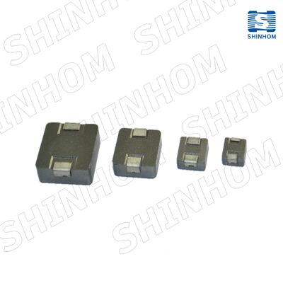
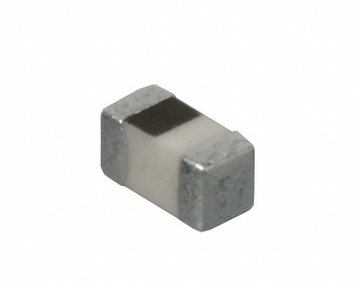
The AIML0402C series ceramic chip inductor uses a multi-layer ceramic structure and closed magnetic circuit design. It offers high self-resonant frequency, low DCR, and anti-crosstalk characteristics, ensuring signal transmission integrity in high-frequency circuits. Inductance range: 1nH to 100nH. The 0402 ultra-small package offers excellent solderability and is suitable for automated SMT placement processes. It is widely used in high-frequency wireless communication, RF modules, Bluetooth devices, GPS, network systems, and computer products.
Multi-layer ceramic structure – stable performance
Closed magnetic circuit – extremely low leakage flux
High self-resonant frequency (SRF)
Low DCR
Anti-crosstalk – signal integrity
Excellent solderability
High reliability – long service life
RoHS compliant – meets environmental standards
High-frequency wireless communication
RF front-end modules
Bluetooth devices
GPS positioning systems
Wireless communication equipment
Network systems
Computer products
Mobile terminal devices
![]()
Q: What are the advantages of the multi-layer ceramic structure compared to wire-wound structures?
A: The multi-layer ceramic structure uses laminated printing and co-firing processes. It offers small size, high consistency, and low parasitic parameters, making it suitable for high-frequency applications. Compared to wire-wound structures, multi-layer ceramic inductors provide higher Q factor and higher self-resonant frequency at high frequencies, with no core saturation issues. They are especially suitable for RF and microwave circuits.
Q: What are the advantages of the closed magnetic circuit design?
A: The closed magnetic circuit confines magnetic flux inside the core. It effectively reduces leakage flux and electromagnetic interference to surrounding circuits, while preventing magnetic coupling crosstalk between adjacent components. In high-density PCB layouts, the closed magnetic circuit design significantly improves signal integrity and system electromagnetic compatibility.